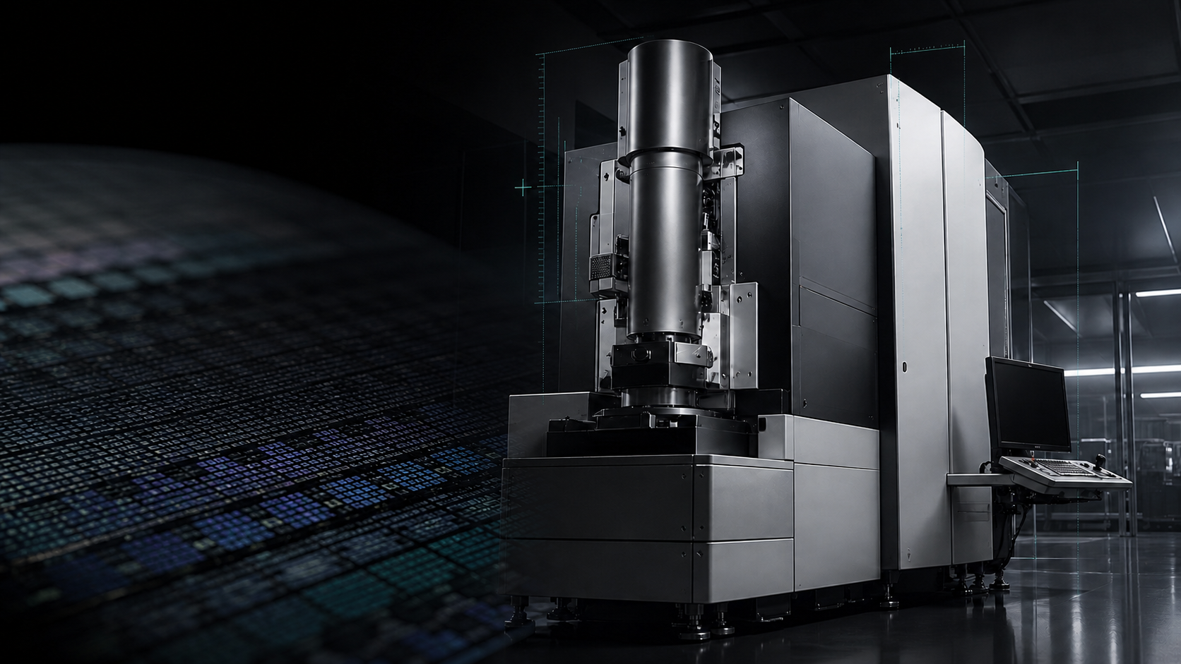
Precision Rebuilt.
Performance Proven.
GCE re-engineers KLA 8xxx CD-SEM systems to meet original factory specifications for the most demanding fab environments.
Wafer Size
3-8" Wafers
Substrates
Multiple
Resolution
4nm
Magnification
400kx
System Configurator
Parameter input: Substrate & Wafer Dimension
grid_view
Substrate Type
data_usage
Wafer Size
Platform Selection
Select model for detailed specifications
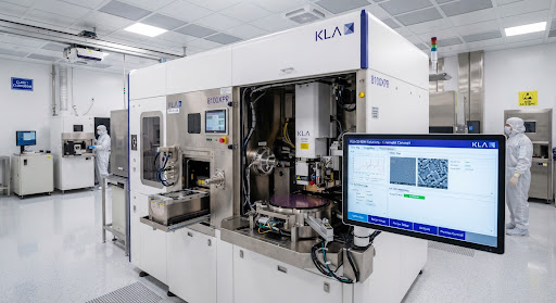
Illustrative comparison profile
KLA 8100XPR
Enhanced resolution and throughput for advanced node monitoring.
Resolution
4nm
Throughput
40 wph
Stage Accuracy
± 1.0 µm
Accel Voltage
200 - 1000V
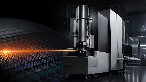
Component Level Tear-down
Every system undergoes a rigorous 240-point inspection. We evaluate vacuum integrity, electron optics, and mechanical stage assemblies against strict OEM baselines. Worn components are not just noted; they are targeted for replacement.
Inspection Points
240+
Vacuum Check
< 10⁻⁷ Torr